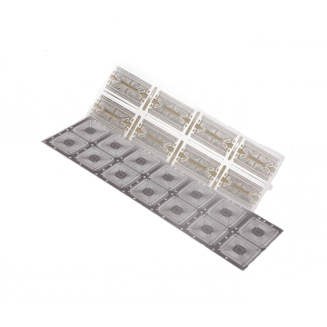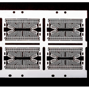

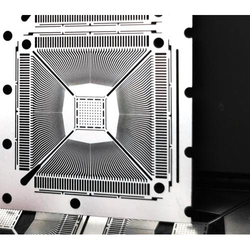
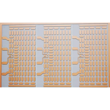
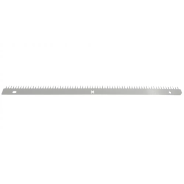
Chemical Etching Lead Frame for Semiconductor
- Min. Order:
- 200 Piece/Pieces
- Min. Order:
- 200 Piece/Pieces
- Transportation:
- Ocean, Air, Express
- Port:
- NINGBO, SHANGHAI
Your message must be between 20 to 2000 characters
Contact Now| Place of Origin: | CHINA |
|---|---|
| Payment Type: | T/T |
| Incoterm: | FOB,CIF,EXW |
| Certificate: | ISO9001:2015 / ISO14001:2015 |
| HS Code: | 8542900000 |
| Transportation: | Ocean,Air,Express |
| Port: | NINGBO,SHANGHAI |
Chemical Etching Lead Frame for Semiconductor
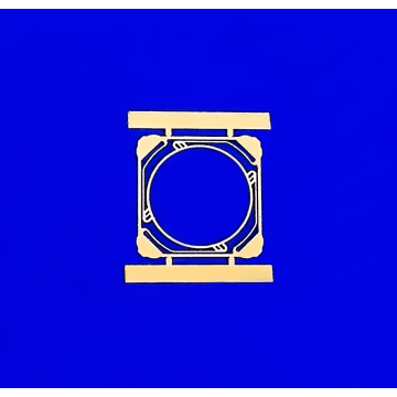
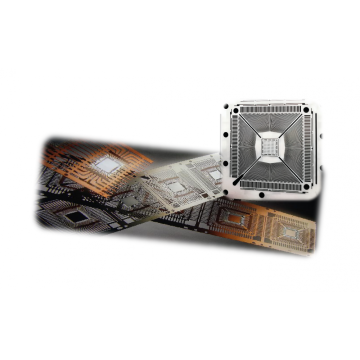
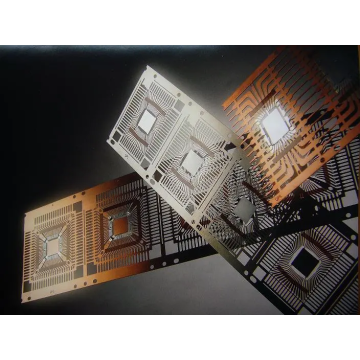
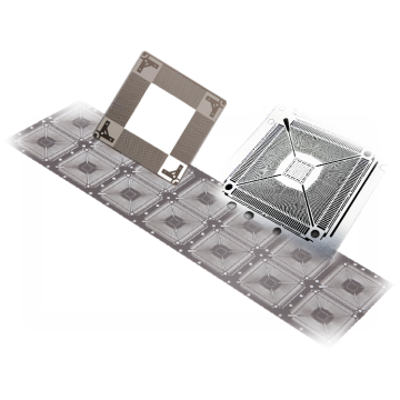
A lead frame is a thin layer of metal frame to which semiconductors are attached during the package assembly process. HEC ‘s lead frames using high precision etching technologies and surface finish technologies, have been used in various applications such as automotive devices requiring high reliability. The raw material use for IC lead frame are copper、copper alloys and iron-nickel alloys. Compared to traditional stamping technology, our chemical etching service can manufacture ultra-fine pitch, high pin count lead frames at a low cost than stamping. Compared to traditional stamping technology, our metal etching service can manufacture ultra-fine pitch, high pin count lead frames at a low cost than stamping. HEC’s multi-pin IC lead frame and ultra-thin products have uniform arrangement, straight etching line and also the half etching product's surface is smooth and delicate.
Below are the specific parameters of this product, please check more IC lead frame in our website for more ideas.
| MATERIAL |
Copper、Copper alloys、 Iron-nickel alloys |
|
THICKNESS |
0.125 - 0.25mm |
| MINIMUM DIAMETER | 0.05 mm |
| MINIMUM DISTANCE | 0.18 - 0.3 mm |
| ACCURACY | +- 0.02 - +- 0.04 mm |
| FINISHING |
Silver、Gold、Palladium、Tin、Nickel plate |

Related Keywords