
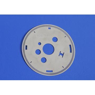
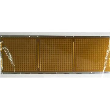
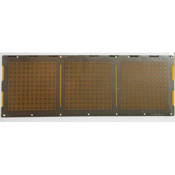
Chemical Etch Thermal Conductivity DBC Ceramic Substrate
- Min. Order:
- 50 Piece/Pieces
- Min. Order:
- 50 Piece/Pieces
- Transportation:
- Ocean, Air, Express
- Port:
- NINGBO, SHANGHAI
Your message must be between 20 to 2000 characters
Contact Now| Place of Origin: | CHINA |
|---|---|
| Payment Type: | T/T |
| Incoterm: | FOB,CIF,EXW |
| Certificate: | IDO9001:2015 / ISO14001:2015 |
| Transportation: | Ocean,Air,Express |
| Port: | NINGBO,SHANGHAI |
Chemical Etch Thermal Conductivity DBC Ceramic Substrate
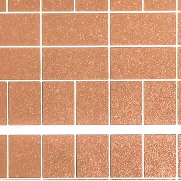
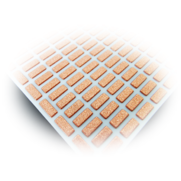
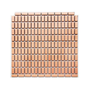
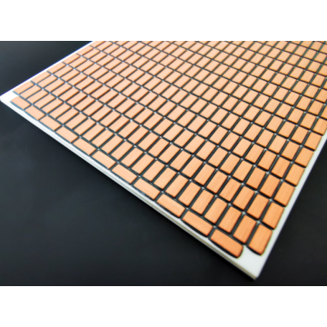
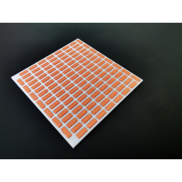
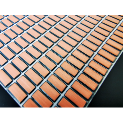
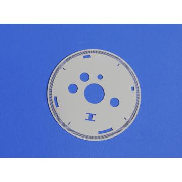
DBC Ceramic Substrate can be applied in various kinds of packaging of electronic module with possibility to etch various kinds of pattern on copper surface. At high temperatures, a copper foil substrate is bonded directly to the surface (single or double sided) of an AI203 OR AIN ceramic substrate. It is a green product without pollution and public harm, which also has a wide range of operating temperature. This substrate has many superiorities, for example, it is highly resistant to vibration and wear, ensuring its long service life. Also, A large number of high-voltage, high-power devices have high requirements for heat dissipation, and ceramic substrates have a better heat dissipation effect. Moreover, it has excellent electrical insulation performance, excellent soft brazability, high adhesion strength and a large current-carrying capacity. It is widely used in many fields, including electronic heater, automotive electronics, aerospace and military electronic element, solar panel element, high-power power semi-conductor module, solid-state relay and many other industry electronic fields.
We custom high precision DBC Substrate with drawings provided by customers. The raw material we use for etched DBC substrate is Ceramic-based double-sided copper clad laminate. We are equipped with professional metal etching equipment and exposure development equipment. Our etching process can achieve double-sided etching of different graphics with 0.3 mm - 0.8mm thickness of copper clad laminate. Also, we can guarantee that our double-sided copper clad laminate substrate is neatly arranged, straight surface line, and have no burr, high product accuracy.
Below are the specific parameters of this product, please check more semiconductor chip carrier in our website for more ideas.
|
Material |
Ceramic-based Double-sided Copper Clad Laminate |
|
Thickness of Copper Clad Laminate |
0.3 mm - 0.8mm |
|
Manufacturing Capacity Minimum Spacing |
0.5 mm - 1.2mm |
|
Manufacturing Capacity Side Corrosion |
0 mm - 0.3mm |
|
DCB Performance Advantages |
Good mechanical strength Good thermal conductivity Coefficient of thermal expansion close to silicon Good thermal stability Good insulation/dielectric strength Possibility to etch various kind of pattern like PCB substrate |
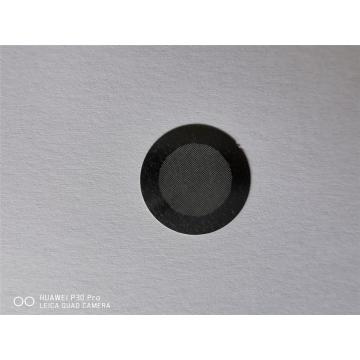
DBC SUBSTRATE PIC

Related Keywords