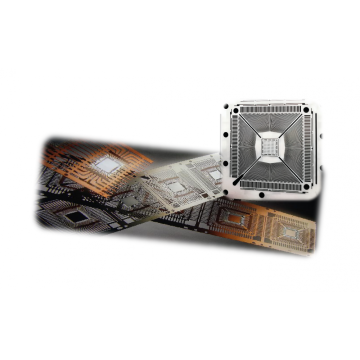
Chemical Etching High Thermal Conductivity DBC Substrate
- Min. Order:
- 50 Piece/Pieces
- Min. Order:
- 50 Piece/Pieces
- Transportation:
- Ocean, Air, Express
- Port:
- NINGBO, SHANGHAI
Your message must be between 20 to 2000 characters
Contact Now| Place of Origin: | China |
|---|---|
| Payment Type: | L/C,T/T |
| Incoterm: | FOB,CIF,EXW |
| Certificate: | ISO9001:2015 / ISO14001:2015 |
| Transportation: | Ocean,Air,Express |
| Port: | NINGBO,SHANGHAI |
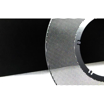
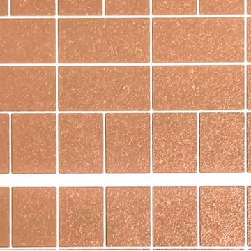
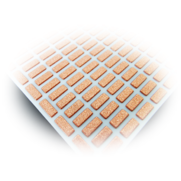
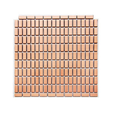
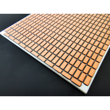
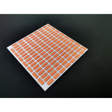
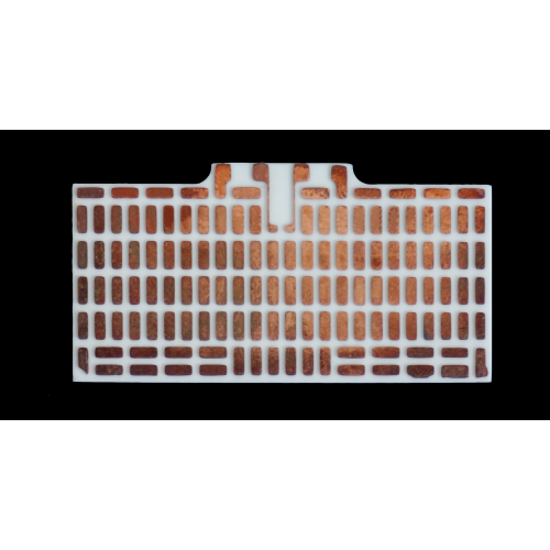
DBC (Direct Bonded Copper) Substrate is a special process board where copper foil is bonded directly to the surface (single or double sided) of and AI203 OR AIN ceramic substrate at high temperatures and can be etched with various graphics. It has excellent electrical insulation performance, high thermal conductivity, excellent soft brazability, high adhesion strength and a large current-carrying capacity. DBC Substrate mainly used in the fields of rail transit, smart grid, new energy vehicles, industrial frequency conversion, household appliances, military power electronics, wind and photovoltaic power generation.
We custom high precision DBC Substrate with drawings provided by customers. The raw material we use for etched DBC substrate is Ceramic-based double-sided copper clad laminate. We are equipped with professional metal etching equipment and exposure development equipment. Our etching process can achieve double-sided etching of different graphics with 0.3 mm - 0.8mm thickness of copper clad laminate. Also, we can guarantee that our double-sided copper clad laminate substrate is neatly arranged, straight surface line, and have no burr, high product accuracy.
Its superiorities of DBC Substrate are as follow:
1. A ceramic substrate with a coefficient of thermal expansion close to that of a silicon chip, which saves the transition layer of Mo chips, saving labour, material and cost.
2. Excellent thermal conductivity, making the chip package very compact, thus greatly increasing the power density and improving the reliability of systems and devices.
3. A large number of high-voltage, high-power devices have high requirements for heat dissipation, and ceramic substrates have a better heat dissipation effect.
4. Ultra-thin (0.25mm) ceramic substrates can replace beo, without environmental toxicity problems.
5. Large current carrying capacity, 100A continuous current through 1mm wide 0.3mm thick copper body, temperature rise of about 17 ℃; 100A continuous current through 2mm wide 0.3mm thick copper body, temperature rise of only about 5 ℃.
6. High insulation withstand voltage, to ensure personal safety and equipment protection
7. New packaging and assembly methods can be realized, resulting in highly integrated products and reduced size
8. The ceramic substrate is highly resistant to vibration and wear, ensuring its long service life.
Below are the specific parameters of this product, please check more semiconductor chip carrier in our website for more ideas.
|
Material |
Thickness of Copper Clad Laminate |
Manufacturing Capacity Minimum Spacing |
Manufacturing Capacity Side Corrosion |
|
Ceramic-based Double-sided Copper Clad Laminate |
0.3 mm - 0.8mm |
0.5 mm - 1.2mm |
0 mm - 0.3mm |
DBC Substrate PIC

Related Keywords